特別講演会のお知らせ(Dr. Ivan Štich)
- 大阪大学共同研究推進プログラムにより、Institute of Physics, CCMS, Slovak Academy of Sciences, SlovakiaのIvan Štich教授を招いて、走査プローブ顕微鏡の理論と実験結果のシミュレーションに関する特別講演会を開催いたします。御来聴を歓迎します。

[1] 特別講演会
題目:Understanding properties of 2D phosphorene from modeling
日時:11月7日(月)10:00 ~ 12:00 (2016年)
場所:応物講義棟2階多目的室 (P1-211)
対象:工学研究科の学生、研究者、教員
[2] 概要
Understanding properties of 2D phosphorene from modeling
by Dr. Ivan Štich: Institute of Physics, CCMS, Slovak Academy of Sciences, Slovakia
Phosphorene is one of the most promising 2D materials, see Figure 1, of enormous current interest. It features bonding markedly different from graphene, strong anisotropy, direct band gaps depending on multi-layer thickness bridging electronic gaps between graphene and transition-metal dichalcogenides, making it suitable for potential applications in photovoltaics, fiber optics telecommunications, and thermal imaging [1]. In addition, the 2D materials can sustain unusually large strain levels compared to their 3D counterparts. Hence, these properties can be used for manufacturing of materials with desired electronic properties via strain and/or layer engineering.
After reviewing some of the properties of single- and multi-layer phosphorene I will show results of our modeling of strain control of vibrational properties in few-layer phosphorene via relatively simple density-functional theory (DFT) approach [2]. As a byproduct of this modeling the electronic states are also calculated which give access to the band-gaps and their dependence on the layer thickness and strain. I will discuss how these results can be used to understand and deduce the phosphorene stack thickness and spatial strain distribution.
Finally, using the ultra-accurate explicitly correlated stochastic Quantum Monte Carlo method [3], I will present what we believe to be the most accurate electronic band gap calculations in single-layer phosphorene [4], see Figure 1, and highlight the challenges encountered if band gap estimates with accuracy higher than 0.1 eV are targeted. I will show the robustness of our benchmark results in comparison with the alternative DFT and GW calculations, both exhibiting significantly larger uncertainties and scatter.
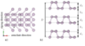
 [Fig.1]
Fig.1 Left: Ball-stick model of few-layer phosphorene. Right: Example of finite-size scaling, up to 3 x 3 supercell, of optical band gap in single-layer phosphorene showing, within the statistical error bars, saturation at around the 3 x 3 supercell. Scaling to 4 x 4 supercell is under way.
[1] A. Castellanos-Gomez, J. Phys. Chem. Lett. 6, 4280 (2015).
[2] K. Tokár, R. Derian, J. Brndiar, and I. Štich, submitted (2016).
[3] W. M. C. Foulkes, L. Mitas, R. J. Needs, and G. Rajagopal, Rev. Mod. Phys. 73, 33 (2001).
[4] R. Derian, T. Frank, L. Mitas, J. Fabian, and I. Štich, in preparation (2016).